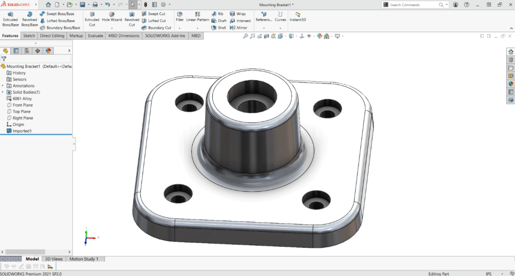
EG R&D

Our Works

We care about every detail of design process from single element to complex structure. Our goal is to meet our valued customers’ product functional and aesthetic requirements

MECHANICAL DESIGN

Product Design and Optimization

  • Enclosure, Assembly, Heatsinking, Artwork, Label, Electro-mechanical part and mechanism designs.
  • User-centered design (Inspiration, Ideation & Implementation)
  • Design Optimization includes Tolerances Analysis, Material Selection, and Design Failure Modes and Effects Analysis (DFMEA).

Engineering Drawings

  • Design tool : SolidWorks and Creo 5.0
  • Create 3D part and Assembly Drawings
  • Design simulation in 3D
  • 2D dimensioning & detailed part drawings.

Product Realization and Safety Certification

  • Plastic Molded, Metal Stamping, Extruded and Casted Enclosures.
  • IPC Standard assembly design.
  • Safety and performance related electro-mechanical designs.
  • DFM for assembly and tooling designs.
  • Various plastic material available such as ABS, PC/ABS, TPU, HDPE, LDPE, PA6, PBT, PC, PET, PMMA, POM, PP, PS, TPE, and etc.
  • BOM Optimization for supply chain availability.
  • IECEx, IEC 60950-1 or/and IEC 60529 (IP 66) compliances.

ELECTRONIC DESIGN

Product Design and Optimization

  • IoT Hardware & IoT sensor designs : Bluetooth 5.2, LTE and WIFI designs using Silab, Quectel, TI, STM, Microchip, Renesas, ADI and MAXIM solutions.
  • Embedded System Design using 8, 16, 32-bit microcontrollers from STM, Microchip and Renesas.
  • Re-engineering services to optimize existing designs for lowering costs.
  • Re-design services to fight obsolescence & semiconductor shortages.
  • DFMEA.
  • IECEx, IEC 60950-1 or/and IEC 60529 (IP 66) compliances.

Embedded System Design – Firmware / Software

  • Development tools : STM32CubeIDE and KEIL
  • Embedded System firmware development based on 8, 16 or 32-bit microcontrollers from STM, Microchip and Renesas.
  • Hardware communication interfaces : I2C, SPI, Ethernet and UART.
  • Mobile module communication using AT commands.
  • Networking based on HTTP and MQTT Protocols.
  • Firmware update through OTA.
  • Support Microsoft Azure IoT Hub

PCB Design

  • Circuit and PCB layout design tools : Altium Designer.
  • Multilayer PCB design up to 8 layers for high speeds application.
  • Rigid and Flexible PCB designs.
  • PCB Layout design rules : IPC2221 standard.
  • IECEx and / or IEC 60950-1 compliances.

Product Realization and Safety Certification

  • Rigid, flexible and / or multilayer PCB fabrication
  • PCBA Prototyping / Mass Production inclusive SMT, AI, Reflow and / or Wave Soldering processes.
  • Box Build
  • Design validation and verification
  • Reliability Test.
  • BOM Optimization for supply chain availability.
  • IECEx, IEC 60950-1 or / and IEC 60529 (IP 66) compliances.

PROTOTYPING

3D PRINTING - FORMLABS 2

Build Volume : 145 x 145 x 175 mm    

Layer Thickness: 20, 50, 100 microns

CNC 3-Axis Machine

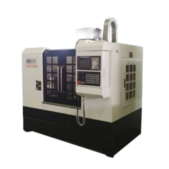
Max Part Size :600 x 860 x 120 mm

Laser Cut Machine

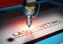
Max. Cutting Size : 600 x 500mm

Max Cutting Thickness : 6 – 10mm

Material able to cut : Metal sheet, Acrylic, Silicon rubber and etc

MANUFACTURING

SMTT Manufacturing Site

After sucessfully created a product, we would send the design to SMTT Manufacturing Site for mass production.